Boost Converter PCB Design - Phil's Lab
Switching boost converter function, working principles, and PCB layout & routing. Best practices, tips, and guidelines to minimise noise, EMI, etc...
[SUPPORT]
Free trial of Altium Designer: https://www.altium.com/yt/philslab
Patreon: / phils94
Mixedsignal hardware design course: https://philslabshop.fedevel.education
Advanced Hardware Design Course Survey:
https://forms.gle/X4jwvtZeJ1jTXh7r9
[GIT]
https://github.com/pms67
[SOCIAL]
Instagram: / philslabyt
[LINKS]
Wiki Boost Converter https://en.wikipedia.org/wiki/Boost_c...
Boost Converter Datasheet https://www.ti.com/lit/ds/symlink/tps...
[TIMESTAMPS]
00:00 Introduction
01:17 Altium Designer Free Trial
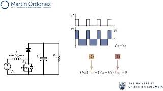
01:43 Boost Converter Basics
04:41 On/Off States
07:36 Input/Output Voltage vs Duty Cycle
08:28 Important Nodes & Loops
09:31 Example Boost Converter Part (Datasheet)
10:40 Schematic
12:17 Datasheet Recommendations
13:18 Layout
19:43 Routing
25:17 Outro


![Buck Converter Circuit Simulation [Altium Designer]](https://i.ytimg.com/vi/VTgiHjXXGL8/mqdefault.jpg)