[EUVL Part1] From the Beginning to HVM
Welcome to our indepth exploration of Extreme Ultraviolet Lithography (EUVL) for patterning on silicon wafers in semiconductor fabrication. Over the course of five episodes, we'll delve into every aspect of this revolutionary technology that is reshaping the modern lithography landscape. In this first episode, we explore the history of EUVL development, revealing insights into its basic working principles, fundamental concepts, and the evolution of the tools and processes used. Below are the main chapters of this video. Click on any timestamp to jump directly to the desired chapter.
1. Introduction to EUVL: From the Beginning to HighVolume Manufacturing (HVM)
[00:00] Introduction: Overview of the EUVL series and expectations for this episode.
2. EUVL Pioneer Works: Discover the early visionaries and groundbreaking experiments that laid the foundation for EUV
[02:55] Xray Proximity Lithography (XPL) in 1985: Targeting 500nm feature demonstration.
[03:30] First Demonstration of EUVL in 1985 by Hiroo Kinoshita.
[07:45] Introduction of MoSi Reflective Mirror to EUVL.
[10:10] Dawn of EUVL: Demonstration of 50nm feature with a synchrotron source.
[11:20] Compact Light Source Development: Using KrF excimer laser.
3. EUVL Early R&D: Explore the initial research and development phases where the potential of EUV began to take shape
[12:25] Renaming to Extreme Ultraviolet Lithography (EUVL) in 1993.
[15:00] Four Pivotal Breakthroughs in Foundational EUVL Research (19811996): Soft Xray imaging, MoSi mirrors, aspherical mirrors, measuring mirror roughness.
[18:45] First Semiconductor Devices Using EUVL: 0.1micron gate length with 10x Schwarzschild microstepper.
4. Consortia R&D / Technology Demonstration: Learn about the collaborative efforts of industry giants to demonstrate and refine this promising technology
[20:25] Global Consortium & Technology Demonstrations: In USA, Japan, Europe, and beyond.
[21:15] EUVL in USA: Intel & EUV LLC Consortium.
[25:45] Prototype Tool Demonstration in USA: Engineering Test Stand (ETS) tool for 200mm wafer process.
[27:15] EUVL in Japan: ASET & EUVA program.
[30:10] Prototype Tool Demonstration by Nikon & Canon in Japan.
[32:10] EUVL in Europe: From EUCLIDES to MEDEA projects.
[34:25] ASML's Alpha Demo Tools (ADT): Sent to IMEC and USA in 2007.
5. Infrastructure Development / Commercialization: Witness the transition from concept to reality as infrastructure is built and EUV moves closer to commercial use
[36:15] EUV Mask Development Led by SEMATECH.
[38:40] Critical Issues in EUV Lithography: Light source, mask, resist.
[40:50] Global Infrastructure for Mask & Resist for EUVL HVM.
6. ASML's NXE:3400B HVM Tool: Delve into the first HighVolume Manufacturing tool, a testament to years of dedication and innovation
[43:10] First EUVL Product: AP chip from Samsung in 2019.
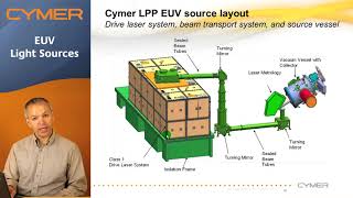
[46:05] Schematics of ASML's NXE:3400B HVM System.
![[EUVL Part2] ASML EUV Light Source](https://i.ytimg.com/vi/LnsuCp1xt3w/mqdefault.jpg)