Master New KiCad 7 In Under 2 Hours |
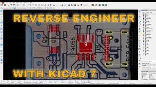
This video is a 2hr compilation of our KiCad Series, which walks through the complete process of PCB development from scratch, while discussing all the important part of PCB Design :
• Learning basic tools and navigation
• Building Schematics
• Performing Electrical Rule Check
• Assigning Footprints
• Understanding PCB Stackup / Netclasses
• PCB Layout
• Routing
• Performing Design Rule Check
• Creating Custom Symbols and Footprint
• PCB Optimization for Production
Download the project files from here : https://github.com/pcbcupid/Kicad7S...
You can directly support us on Pateron : / pcbcupid
If you like to learn what is PCB You can check out our website PCB CUPID:
https://pcbcupid.com/
If you have any question or doubts regarding this video, You can drop your questions here : https://pcbcupid.com/questions/
Make sure to subscribe and share this content with someone who would love this!
▬▬▬▬▬▬ Follow us on other social media platforms! ▬▬▬▬▬▬
Instagram: / pcbcupid
LinkedIn: / pcbcupid
Twitter: / pcbcupid
Pinterest: / pcbcupid
Reddit: / pcbcupid
▬▬▬▬▬▬ Contents of this video ▬▬▬▬▬▬
0:00 intro
0:15 Introduction to KiCAD
4:13 KiCAD UserInterface
9:48 Schematic
16:45 Prettify Schematic
22:00 Electrical Rules Check
26:22 Footprint Assignment
38:42 Understanding PCB Stackup
46:05 Predefined Rules & Constraints
56:58 PCB Layout
01:04:42 Routing
01:13:30 Design Rule Check
01:23:42 Gerber File Generation
01:31:00 Custom Symbol
01:41:07 Custom Footprints
01:49:13 PCB Optimization
#pcb #learn #printedcircuitboard #kicad #electronic #cad #pcbdesigning #howto #begineer #electrical #stackup #fotoprint #custom #design #optimization #tutorial


