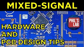
Practical RF Hardware and PCB Design Tips - Phil's Lab #19

Some tips for when designing hardware and PCBs with simple RF sections and components. These concepts have aided me well when designing 4layer embedded systems PCBs.
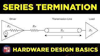
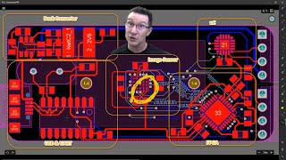
Topics: critical trace lengths, stackups, controlled impedance traces (microstrip, stripline), impedance discontinuities due to wide pads, clearances, bias tees.
Visit https://jlcpcb.com/RHS for $2 for five 2layer PCBs and $5 for five 4layer PCBs.
Open Seneca: https://openseneca.org
Git: https://github.com/pms67
If you're enjoying my content, please consider becoming a patron:
/ phils94
[TIMESTAMPS]
00:00 Introduction
00:27 JLCPCB
00:53 Overview
02:08 Critical length
06:45 Stackup
08:51 Controlled impedance traces
12:34 Impedance discontinuities (padtotrace)
14:34 Clearance
15:17 Antenna bias tees
ID: QIBvbJtYjWuHiTG0uCoK