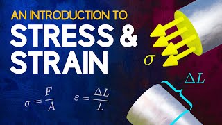
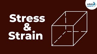
[Thin Film Part1] Stress and Strain

Welcome to the "Thin Film Series," your gateway to understanding the fundamental materials and processes in semiconductor devices. In this inaugural episode titled "Thin Film Stress & Strain Engineering," we dive deep into the latest advancements in thin film technology and their critical impact on semiconductor manufacturing. Join us as we explore how thin film stress and strain engineering affect wafer warping and learn about the methodologies employed to mitigate these effects. This video is designed to equip you with a thorough understanding of the crucial role that thin film stress and strain engineering play in the fabrication of semiconductor devices. Whether you're an aspiring engineer, a seasoned industry professional, or simply a semiconductor enthusiast, this episode will offer valuable insights into the complex world of thin films. Don’t forget to like, subscribe, and turn on notifications for our channel to stay updated on all our educational content. Below are the main chapters of this video. Click on any timestamp to jump directly to the desired section.
Episode Outline:
1. Wafer Warping: Analyzing Causes and Mitigation Strategies
[1:08] Overview of Wafer Warping: Types and phenomena.
[2:43] Impacts on Semiconductor Manufacturing Risks associated with wafer breakage during Electrostatic Chucking (ESC).
[4:30] Wafer Warping in Photolithography: Risks of defocus and overlay errors after vacuum chucking.
[6:18] Challenges in 3D NAND Manufacturing: Issues caused by thick Oxide/SiN layers.
[7:55] YTMC's Xstacking: Addressing wafer warping in wafer bonding integration.
2. Stress Measurement: Techniques and Applications
[10:29] Measuring Wafer Warping: Techniques for blank silicon wafers.
[12:24] Stoney Methods for Stress Measurement: Application in convex or concave warping.
[14:09] Film Stress Management: Addressing stress arising from coefficient of thermal expansion (CTE) disparities.
[16:45] Bow Height Measurement: Using the Stoney method.
[18:14] Thermal Stress Curves of Thin Film: Interpreting stress changes postdeposition.
[20:37] Advanced Wafer Warping Measurement: Employing PWG scanners for complex cases.
3. Thin Film Stress: Ripple, Crack, and Delamination
[22:02] Impact of CTE on Thin Film Stress and Wafer Warping.
[23:46] Controlling Thin Film Stress: Stress characteristics of common semiconductor films.
[25:22] Stress Impact on Thin Film Defects: Ripple, crack, and delamination.
[27:10] Intrinsic Stress in Thin Film Deposition: Stress from material properties.
[29:00] Stress Relief Layers in STI Integration: Addressing stress issues in device integration.
4. MOSFET Strain Engineering
[30:17] Enhancing MOSFET Performance via Strain Engineering.
[31:33] Strain Enhanced Mobility: How strain alters channel mobility.
[33:45] Local Strain Engineering in MOSFETs: Overview of techniques based on process and material.
[35:53] Strain Engineering in pMOS and nMOS Devices: Techniques and challenges.
![[Thin Film Part2] Vacuum Basics](https://i.ytimg.com/vi/0mz4Tvrclj4/mqdefault.jpg)